The charge amplifier requires a high input impedance and a low bias current.
An operational amplifier. A high input impedance avoids electricity on the feedback capacitance.
The charge leakage, low bias current prevents excessive charge and discharge from the feedback capacitor. charge
The layout of the amplifier circuit is the key. The operational amplifier shell must be well connected
The input end of the ground should be well protected and well connected to the same place as the shell.
The layout of the protected input side is shown in Figure 46. To prevent operation amplifier
The leakage noise caused by the large insulation is applied to the end connection of the insulated STANDOFF joint
Enter the cable.
In spite of the above protection measures, the output voltage is still drifting. For compensation drifting
Shift, usually in a circuit, to design a reset switch at one end of one end with a manual
Put the output to zero. One is to connect a reed switch on the resistance, but
The feedback capacitor is Cf parallel. The starting reed switch closes the switch and releases the switch.
Feedback the voltage in the capacitor.
Another method is to use a MOSFET device to determine the minimum gate voltage of the FET in the device with the maximum output voltage and the closing voltage. In practical applications, the MOSFET gate is given a voltage greater than the amplifier voltage to reduce its leakage / source impedance and to create a current path for the feedback capacitance discharge.
The third method is in the feedback loop and a voltage divider. This electricity
A time constant (CfRf) is generated, and the time constant and film capacitance
It is independent and can be controlled accurately.
Figure 47 the signal level detector applied in high SNR. this
It is ideal for a circuit to detect impact in low level vibration. Signal to noise ratio
A situation of low and necessary identification of shock or pressure signals from a background vibration.
The differential amplifier circuit of figure 48 is suitable. This circuit consists of two
A sensor that drives a differential amplifier.
This circuit uses the concept of common mode suppression. The two switch mechanical coupling is used
Eliminate the unwanted vibration of the analog two. Input or input on a switch
The pressure signal produces the output, while the other is not.
The CMOS logic circuit provides a low level of interface with the piezoelectric film.
This program. As mentioned earlier, the low energy consumption circuit implemented by CMOS technology is very important.
It is suitable for piezoelectric thin film switches. CMOS applications for piezoelectric thin films
It's working on low frequency. Other features to be considered include the input leakage of the device
Flow, input impedance, input bias impedance, and EMI effect. For example, one
The CMOS circuit can be used to induce a single impact or a pressure signal.
The D flip-flop of figure 49 shows that an impact or pressure signal will drive one
Sound alarm.
The circuit diagram of 50 in counting application induction of repeated impact or pressure
Signal.
There are many different CMOS circuit configurations available to the piezoelectric film interface.
The common point of all circuits is that the input bias resistance and the piezoelectric film are in parallel.
The resistance is connected in series with the piezoelectric film. The bias resistor is responsible for the leakage current and the series of electricity
The hindrance current protects it from the shock of the electric charge of the electrostatic discharge.
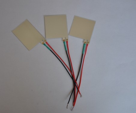
Cable
In the application of the amplification circuit that is not possible near the piezoelectric thin film sensor, the connection cable which can transmit high resistance signal must be considered.
Shielded coaxial cables are used to reduce noise, resulting in cable leakage and additional capacitance. In most cases, the initial insulating layer of the cable has a high impedance, and the non polarized plastic such as high purity polyethylene or Teflon PTFE. As the movement of the cable generates noise, it interferes with the transmission of the signal, making the cable not.
The state of vibration is also important.
Manufacture
The membrane of the piezoelectric membrane is produced in the purifying room. First, the PVDF pellets are melted and extruded into sheets, and then further extend to the thickness of the extruded sheet 1/5. The extension of the temperature of the melting point of the polymer causes the chain of molecules to become a parallel crystalline surface, called "beta phase". In order to obtain high level piezoelectric activity, the polymer of beta phase is placed in a very high electric field, so that the crystal is aligned with the polarization field. The PVDF copolymer can be polarized without extension.
The thickness of the metallized layer, which is deposited by evaporation, is usually 500~1000A, and almost any metallized layer can be deposited so. The commonly used metals include nickel, aluminum, copper, gold and its alloys. The fabrication of electrodes is a mask spray or a continuous metallization of chemical etching with photoresist. The resolution can reach 25 m linewidth, the conductive silver ink screen printing electrode, the electrode is much thicker, about 5~10 m, this method used for the electrode of multi sensors and complex shapes in monolithic material. Silver layer is bonded to a thin layer, and capacitive coupling and piezoelectric film. Each electrode has its own advantages and disadvantages.
In general, spray metal is used for high resolution arrays, low heat quality thermoelectric applications, or inert medical applications. The fully metallized sheet can be carefully cut with a razor blade, and it will not cause a short circuit in the direction of the film. Screen printing ink is very strong and flexible, and it can withstand high stress (>10%). It can also be used under high voltage conditions without breakdown and suitable for continuous printing. However, because of cutting off components from screen printing electrodes, it is very likely that the thick piezoelectric film will be short circuited in thickness direction, so the non metallized edges should be kept. The electrode layer limits the response of piezoelectric film to external stress and strain on the membrane plane mechanically, but it is very useful for working in the direction of thickness mode.
After metallization, the final product will be produced after many processing steps. In short, a piezoelectric film is laminated on a protective carrier film, formed by cutting and packing with a lead or terminal, and sometimes a signal finishing circuit. Sensor parts after encapsulation
|