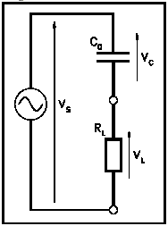
Basic circuit principle
A reasonable design of the interface circuit will play a key role in the optimization of the piezoelectric film sensor. The application of piezoelectric film from toys to military sensor. The interface circuit and the application are closely related. In many applications, a piezoelectric film can be directly connected to an electronic circuit without a special interface. But for applications that require an interface circuit, it is suggested that the following three steps be taken into consideration:
1. in the desired dynamic range, the frequency range and signal are considered.
Range requirements.
2. select the appropriate load resistance to ensure the low end working frequency and
The signal loss caused by the load effect is minimal.
3. if the signal level is very low, a buffer circuit is selected. If needed
To a high value of load resistance (such as 22M or above), select a
A buffer amplifier with low leakage and high impedance. Market is sold for buffering
The JFET or CMOS operational amplifier of the circuit.
Simplified equivalent circuit
The first step in the design of the interface circuit is the characteristics of the piezoelectric film
It is understood as part of the equivalent circuit. Figure 34 shows the piezoelectric film
A simplified equivalent circuit. It is connected by a voltage source with a phase.
The capacitance of the piezoelectric film is expressed in series capacitance Cf, and it is with the film.
The dielectric constant is proportional to the area, but inversely proportional to the thickness of the membrane. Voltage
The amplitude of the source is equal to the open circuit voltage of the piezoelectric film, according to the size of the excitation.
The change is different, ranging from a few microvolts to more than 100 volts. equivalent circuit
It is suitable for most applications, but for an ultrasonic vibration at high frequency.
When the little significance.
Figure 35 gives an equivalent circuit for a charge generator.
The film capacitance Cf and internal resistance Rf are given in the equivalent circuit. As before
The induction charge Q is linear to the added force, and the capacitance is Cf
It is proportional to the surface area of the membrane, but inversely proportional to the thickness of the membrane. When applied to
In the case of low frequency, the internal resistance Rf is very high and can be ignored. open circuit
The output voltage can be obtained by the membrane capacitance, that is, V = Q / Cf.
Input resistance
The key part of the interface circuit is the input resistance. The input resistance affects the ability of low frequency measurement and the amplitude of the signal. This is called the "load effect".
The piezoelectric film capacitance can be considered as the equivalent source impedance. The source impedance will increase with the decrease of the membrane capacitance and the decrease of the working frequency. It is important to note that this point is important. The source impedance is combined with the input resistance to form a divider. With the decrease of the ratio of the input resistance to the source impedance, the total output voltage decreases. Therefore, selecting the appropriate input resistance for the electronic interface is the key to minimize the load effect.
time constant
In addition to the input resistance, the input capacitance of the interface circuit is the same.
The impact on the output. The equivalent circuit of a piezoelectric film is given in Figure 36.
The input resistance is Ri, and the input capacitance is Ci. Typical time of a piezoelectric film
The domain response is shown in Figure 37. The charge produced after the addition is Ri (Cf+Ci).
The determined time constant attenuates.
The time constant indicates that a signal attenuates to its original amplitude.
The time required for 70.7% (~3dB). The smaller the time constant, the letter
The faster the number attenuates. Because of this limited time constant, piezoelectric thinning
The film is only suitable for dynamic measurement, not static measurement (minimum 0.001Hz).
If a long time constant is required, high input power can be used
Resistance and film capacitance. However, it is necessary to know that high input resistance will also be higher.
The noise needs to be compensated by shielding.
frequency response
Another important aspect of the time constant is the equivalent circuit
In the frequency response, the equivalent circuit has a RC as shown in Figure 38.
High pass filter characteristic curve. The vertical axis indicates the measured output signal and production
The ratio of the raw signal (the open circuit voltage of a piezoelectric film). 0dB indicates no
Signal loss, and the cut-off frequency (below 3dB) is opposite to the time constant
When a piezoelectric film sensor works below the cut-off frequency,
Its output signal will be greatly reduced. In low frequency measurement, the input resistance is required
Be high enough so that the cut-off frequency is obviously lower than the required work.
Frequency. This can be realized from the time constant and the load effect.
A goal.
As an example, figure 39 gives a shielded piezoelectricity.
The frequency response of a membrane sensor (SDT1 type). In an example, SDT and one
A circuit of 10M load resistance and a FET. Piezo membrane
The capacitance is 2.4nF, the load resistance is 10M, so the time constant
The number is 24 milliseconds, so its cut-off frequency is 6.6Hz. For contrast
If, instead of 10M load resistance resistance 100M, cut
The stop frequency is reduced to 0.66Hz. This sensor element can work in any application above the cut-off frequency determined by the resistance value.
When the circuit can not be placed near the sensor, it is recommended to add a buffer circuit near the sensor. The buffer circuit changes the high output impedance of the piezoelectric film device to the low output impedance, thereby causing the signal loss and noise in the cable.
Reduce to a minimum. For large size (high capacitance) piezoelectric film sensors, even small signals and long cables may not require a buffer circuit. |